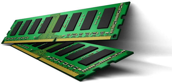
STEC | DRAM Memory | DDR3, DDR2, DDR, SDRAM, EDO FPM, Motherboard Qualifications
 
STEC | Advanced OEM SSD and Memory Solutions | WELCOME
RELATED PRODUCTS
  DDR3
  DDR2
  DDR
  SDRAM
  EDO/FPM
  Motherboard Qualifications
Home > Interface > DRAM > DRAM Education
 DRAM TECHNOLOGIES
 EDO/FPM
FPM (Fast Page Mode) and EDO (Extended Data Out) technologies are older technologies popular in the late 1980's and early 1990's. These technologies should not be used for new designs, but STEC can still provide many modules using these technologies for older designs that may still be in production or for replacement parts for customer's systems that are installed in the field.
 SDRAM
SDRAM (Synchronous DRAM) is the common term to classify PC66 (1997), PC100 (1998) and PC133 SDRAM (1999/2000). SDRAMs are based on standard dynamic RAM chips, but have sophisticated features that make them considerably faster. First, SDRAM chips are fast enough to be synchronized with the CPU's clock, which eliminates wait states. Second, the SDRAM chip is divided into two cell blocks, and data is interleaved between the two so that while a bit in one block is being accessed, the bit in the other is being prepared for access. This allows SDRAM to burst the second and subsequent, contiguous characters at a rate of 10ns, compared to 60ns for the first character. SDRAM chips use a power supply voltage of 3.3 volts.
 DDR
Double Data Rate (DDR) is an advancement over SDRAM technology that increases memory bandwidth and performance while maintaining competitive pricing. DDR is the evolutionary technology that succeeded the previous standard Synchronous DRAM technology, which is now called SDR (Single Data Rate). DDR achieves its performance by transferring data on both the rising edge and the falling edge of the clock. Standard speeds for DDR include PC-2100 (7.5 ns clock), PC-2700 (6.0 ns clock), and PC-3200 (5.0 ns clock). Chips with DDR technology also save power because they run at 2.5 or 2.6 volts rather than the higher voltages used by the earlier technologies.
 DDR2
DDR2 is an evolutionary enhancement over DDR. This technology is currently the largest selling technology today and offers the best cost per bit. Most new systems designs today would likely choose to use DDR2. It takes advantage of the DDR improvements to transfer data on both edges of the clock. However, it further improves the speeds to provide standard transfer rates of PC2-3200 (5.0 ns clock), PC2-4200 (3.75 ns clock), PC2-5300 (3.0 ns clock), and PC2-6400 (2.5 ns clock). DDR2 chips save further power over the previous technologies because these chips use a standard voltage of 1.8 volts.
 DDR3
DDR3 continues the evolution of the double data rate technologies to provide continued improvements in performance. The DDR3 technology is just being introduced and is not projected to be cost competitive with the DDR2 technology until 2009 or 2010. However, it does offer increased transfer rates of PC3-6400 (2.5 ns clock), PC3-8500 (1.875 ns clock), PC3-10600 (1.5 ns. Clock), and PC3-12800 (1.25 ns clock). So system designs that are performance driven may want to start looking at this technology. DDR3 also saves power by lowering the power supply voltage to 1.5 volts.
 Motherboard Qualified Memory
In order to ensure that there are no compatibility problems when using STEC DRAM modules with Intel motherboards, STEC will qualify certain modules at CMTL (Computer Memory Test Labs) on certain Intel motherboards. For those customers using those motherboards, this will ensure full compatibility and minimize technical issues. Motherboard Qualified Memory can potentially be any technology type or form factor. These modules do have a fixed bill-of-materials which STEC will not change without first resubmitting the new BOM to CMTL for re-qualification.
 SPECIALIZED FORM FACTORS
 Full-Sized DIMMs
The full-sized DIMM form factor was the original form factor that was created for DRAM modules. It is in wide use with desktops, servers, and systems used in embedded and telecommunications applications. This module is 133.5 mm wide and is 30 mm or more tall. Standard full-sized DIMM form factors have been defined with pin counts of 168 (SDRAM), 184 (DDR), and 240 (DDR2 and DDR3).
 Very Low Profile (VLP) DIMMs
The Very Low Profile (VLP) DIMM was created to save height for space constrained systems, including blade servers and ATCA (Advanced Telecommunications Architecture) applications. The DIMMS are also 133.5 mm wide and have the same pinout as the DDR, DDR2, and DDR3 full-sized DIMMs. However, these modules will typically have a height between 18-19 mm. This shortened height allows the designer to use a vertical socket and still fit the DIMM into his constrained chassis space.
 So-DIMM
The So-DIMM is a shortened DIMM form factor that was created originally for use in notebook computers. This module has a width of 67.6 mm and these will typically use a horizontal socket when designed into the system. The original So-DIMM was defined without ECC for use in notebooks. But additional versions that include ECC have been created for embedded, telecomm, and other applications that require additional reliability. The So-DIMM can come in versions with pin-counts of 144 pins (SDRAM), 200 pins (DDR and DDR2), and 204 pins (DDR3).
 Mini-DIMM
The mini-DIMM is a relatively new form factor that was invented to provide the benefits of a shortened DIMM length but still provide additional pin-count to support new features in the DDR2 technology. Mini-DIMMs are currently available for only DDR2 in a 244-pin module and will always include ECC. These modules are 82 mm long. It is likely that future extensions to the DDR3 standard will also provide this form factor for DDR3 technologies.
 VLP Mini-DIMM
The VLP mini-DIMM is a new form factor that combines the shorter length of the mini-DIMM with the shorter height of the VLP DIMM. This form factor is a good solution for highly space constrained systems that only need a small to moderate amount of memory. The typical size of a VLP mini-DIMM is 82 mm long with a height between 18-19 mm.
 CONFIGURATION OPTIONS
 Error Correction Code (ECC)
The most common widths of DRAM modules are either 64 or 72 bits wide. The ECC option refers to a module that is 72 bits wide. The 72 bits can be split into 64 data bits and 8 check bits. These modules work with chipsets that support Error Correction Codes which will provide additional reliability in the memory system. These codes can detect and correct one bad bit within the 64 bit data word and they can detect two or sometimes more than two bad bits. Modules with ECC are most commonly used in server or telecomm applications where reliability and uptime are extremely important.
 Non-ECC
Non-ECC modules are normally 64 bits wide. These modules do not provide any error detection or correction capabilities. They are typically used in single user desktop or notebook systems. Because these systems only service one use and do not require 24/7 operation, the standard reliability built into DRAM modules is adequate for these systems.
 Registered DIMM (RDIMM)
In large systems that use a lot of memory, there may be as many as 4 or 8 DIMM modules attached to the chipset over a single memory channel. Because of the heavy electrical load it may be difficult for the chipset to send out the Address and Command signals with enough strength to directly drive all the DRAM chips on all the modules and meet the speed requirements. For this reason, these types of systems will normally use Registered DIMM modules. These modules put a special chip on the DIMM, called a Register chip. This chip receives the Address/Command signals from the chipset and receives it into a latch. On the next clock cycle the Address/Command signals are then sent out to the DRAM chips from the Register instead of directly from the chipset. The advantage of this arrangement is that the Register presents just a single input load to the chipset instead of the 9 or 18 or 36 loads that the chipset would see when driving the DRAM chips directly. This can allow the interface logic to run at higher speeds. Registered DIMMs are often used in servers and other applications that use a lot of memory. Registered DIMMs will always be configured with ECC.
 Unbuffered DIMM (UDIMM)
A DIMM module that does not have a Register is called an Unbuffered DIMM. These modules are satisfactory in small systems that have only one or two DIMM modules per channel. The chipset Address/Command signals have enough drive to directly drive all the DRAM chips without compromising on the bus speed. Unbuffered DIMMs are most often used in desktop and notebook systems which will only have two or four DIMM slots in the system. Unbuffered DIMMs can be configured either with ECC or without ECC.
 Fully Buffered DIMM (FB-DIMM)
The FB-DIMM is a new memory architecture that was recently introduced for use with Intel server chipsets. This architecture was designed for very large memory systems that may have as many as eight or sixteen DIMM sockets per channel and four or more memory channels. The FB-DIMM uses an advanced chip on the DIMM called the Advanced Memory Buffer (AMB). This chip not only buffers the Address/Command signals, like a Register chip, but it also buffers the outputs of the DRAM chips. The AMB chip also provides for a parallel to serial conversion and transfers the data to the chipset or other FB-DIMMs using a very high speed serial protocol. The FB-DIMM architecture is also characterized by a daisy-chain architecture and transfers the data from the chipset to the first FB-DIMM and then from the first to the second, second to the third, etc. This point-to-point connection has low loading which is needed to support the transfer rates on the very high speed serial bus. All FB-DIMMs are configured with ECC.


IN THIS SECTION
DRAM Education
Specialized Form Factors
Configuration Options
DOWNLOAD CENTER
DATASHEETS
DDR3 Datasheets
DDR2 Datasheets
DDR PC3200 Datasheets
DDR PC2700 Datasheets
DDR PC2100 Datasheets
SDRAM PC133 Datasheets
SDRAM PC100 Datasheets
BROCHURES
DRAM Family
SPREADSHEETS
DRAM Decoder
DRAM Part Number Generator
CERTIFICATE & COMPLIANCE
RoHS Certification
CONTACT INFORMATION
DRAM Team
3001 Daimler Street
Santa Ana California 92705
Tel (949) 476-1180
Email DRAM@stec-inc.com
Sitemap  | Global Contacts & Support  |   Locations  |  Investor Relations  |  Environmental Leadership
Terms and Conditions  |  Privacy Policy  |   Warranty Terms
Copyright ©2007 STEC Inc. All Rights Reserved.